A team of researchers at Columbia University has developed a pioneering method to enhance nonlinear optical effects at the nanoscale. Led by Jim Schuck, a professor of mechanical engineering, the researchers have successfully etched metasurfaces into ultrathin crystals to significantly boost their optical performance. This advancement, detailed in a paper published in Nature Photonics in October, represents a significant leap in the field of quantum technology.
The team’s research centers around transition metal dichalcogenides (TMDs), a class of crystals that can be peeled into atom-thin layers. These layers have shown promise in generating entangled photon pairs, a vital component for quantum applications. Schuck and his team overcame limitations associated with conventional nonlinear crystals, which are often bulky and inefficient. As Chiara Trovatello, the corresponding author of the study and an assistant professor at Politecnico di Milano, noted, “Size doesn’t matter for something like a laser pointer that you’ll hold in your hand. But for quantum technologies, size becomes crucial.”
In their earlier work published in January, the researchers used a technique called periodic poling to produce photons capable of powering qubits. This involved layering a TMD called molybdenum disulfide in alternating orientations to optimize its optical output. The layers were carefully arranged to ensure that the light waves remained phase-matched, preventing interference.
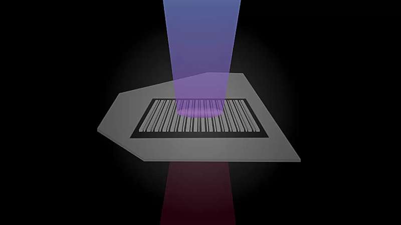
The latest research introduces a complementary approach through the use of metasurfaces. By etching artificial geometries into the surface of the crystals, the team was able to create new optical properties that significantly enhance their functionality. Ph.D. student and first author Zhi Hao Peng developed a straightforward nanofabrication technique that etched repeating patterns onto a molybdenum disulfide flake. His innovative design improved second-harmonic generation—where two photons merge to create a photon with double the frequency—by nearly 150 times compared to unpatterned samples.
The implications of this research are profound for quantum technologies, particularly as the demand for smaller, more efficient qubit sources increases. Current qubit sources occupy significant space, often requiring entire rooms, but the new methods could lead to compact, on-chip quantum photonics. “With our footprint, we can really start to think about fully on-chip quantum photonics,” Schuck remarked.
The team’s theoretical collaborators, including Andrea Alu from the CUNY Advanced Science Research Center, assisted in determining the optimal metasurface pattern to enhance the nonlinear response of TMDs. Their findings suggest that a simple modification can lead to complex behaviors that significantly boost optical efficiency across ultrathin path lengths.
As the researchers continue to refine their techniques, they aim to explore the reverse process of photon generation, working towards splitting one photon into two entangled photons. This could further propel the development of scalable quantum technologies.
The study not only highlights the remarkable potential of metasurfaces in photonics but also establishes a foundation for future innovations in quantum systems. As technology advances, the integration of these nanoscale devices into existing telecommunications infrastructures promises to revolutionize how quantum information is processed and transmitted.
For further information on this groundbreaking research, the full study can be accessed in the Nature Photonics journal.